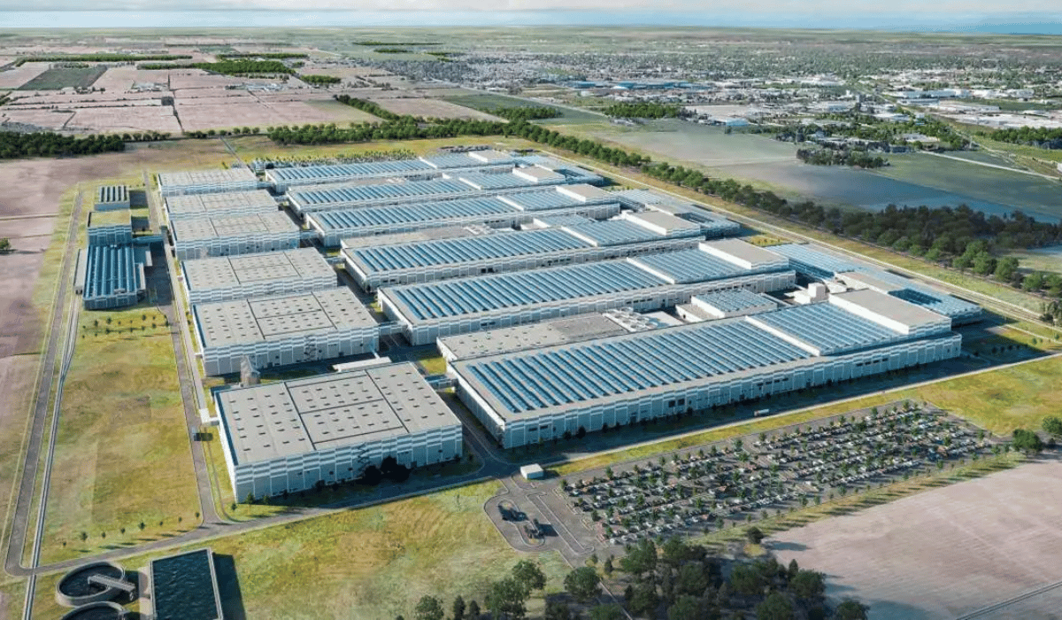
Prime Minister Narendra Modi and Uttar Pradesh Chief Minister Yogi Adityanath on Saturday, February 21, laid the foundation stone for a 3,700 INR-Crore semiconductor facility in Noida. The project marks a major investment under the state’s electronics manufacturing expansion.
The semiconductor unit will be developed by a joint venture between HCL Group and Foxconn. The facility will come up on an anticipated 48 Acres of land in the Yamuna Expressway Industrial Development Area. Moreover, the Noida semiconductor facility will focus on manufacturing display driver chips with a capacity of 20,000 wafers per month. These chips will be used in mobile phones, laptops, automobiles, and other electronic devices. The unit will further support domestic electronics manufacturing.
Also Read: Economic Survey 2026: Key Insights and Growth Outlook for the Industrial Sector
The facility will add to semiconductor fabrication infrastructure in Uttar Pradesh. Moreover, it will strengthen the electronics manufacturing cluster emerging in the YEIDA region. The project represents a significant addition to the state’s semiconductor infrastructure pipeline.

Biltrax Construction Data is tracking 38,000+ projects on their technology platform for their clients.
Get exclusive access to upcoming projects in India with actionable insights. Furthermore, gain a competitive advantage for your products in the Indian Construction Market.
Visit www.biltrax.com or email us at contact@biltrax.com to become a subscriber and generate leads.
Disclaimer: The information herein is based upon information obtained in good faith from sources believed to be reliable. All such information and opinions can be subject to change. Furthermore, the image featured in this article is for representation purposes only. It does not in any way represent the project. If you wish to remove or edit the article, please email editor@biltrax.com.
Discover more from Biltrax Media, A Biltrax Group venture
Subscribe to get the latest posts sent to your email.